
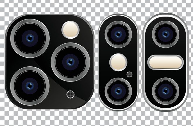
The future of mobile photography is about to be radically redefined with the introduction of metal lenses. These revolutionary lenses, made through advanced lithographic nanoimprinting techniques on silicon substrates, are on the verge of making conventional optical lenses obsolete.
Their integration into chips promises not only a significant reduction in production costs but also a qualitative leap in the efficiency and precision of digital photography. In 2024 we will see robust progress in this direction.
The revolutionary potential of metalents
Metallens technology represents a breakthrough in the field of mobile photography. Unlike traditional lenses, which are made using laborious processes that include casting, grinding and polishing glass or plastic, metal lenses are etched onto a sheet of silicon dioxide or similar material. This innovative process uses silicon pillars the size of the wavelength of light, which interact with it to bend and disperse it in precisely controllable ways.
Shall I try to explain it in much simpler ways? Forgive the approximation.
Metalents are like thin, transparent sheets with very small pillars printed on them, invisible to the naked eye. These pillars are so small that they are the same size as the colors of light. When light passes through the sheet with these pillars, it is bent and directed as in a normal lens. So instead of having to make complex and expensive glass lenses, we can simply “print” these pillars onto the sheet, making them perfect for devices like smartphones.
Metalenti, not an easy road
Despite initial efforts, the fabrication of metalents via light-based lithography has encountered significant obstacles. The team of Andrew McClung at the University of Massachusetts at Amherst has overcome these limitations by developing a method compatible with large-scale chip production.
Researchers have perfected a technique called lithographic nanoprint, which prints the design of the metal elements onto a resin called polymethyl methacrylate (PMMA), placed on top of a layer of silicon nitride and a substrate of silicon dioxide. If you want to learn more, I'll link the research here.
Applications beyond photography
In addition to mobile photography, metal lenses have potential applications in various fields. They can be used to channel light through chips, creating complex 3D designs for optical processing.
These lenses could also find use in webcams and other similar devices, as well as in highly efficient and compact optical systems that can be integrated into a wide range of applications.
Future challenges and prospects
Metal lenses enter the market with the promise of bringing a more efficient and less expensive technology compared to traditional lenses. There is obviously work to be done on the scalability and integration of this technology into current production processes. McClung and his team's research marks an important step toward overcoming these barriers, bringing us ever closer to introducing metalents into mass-market consumer devices.
With their unique properties and innovative manufacturing process, metal lenses will enable a new era of incredibly more efficient and compact devices. We can't wait to take the next photograph.